

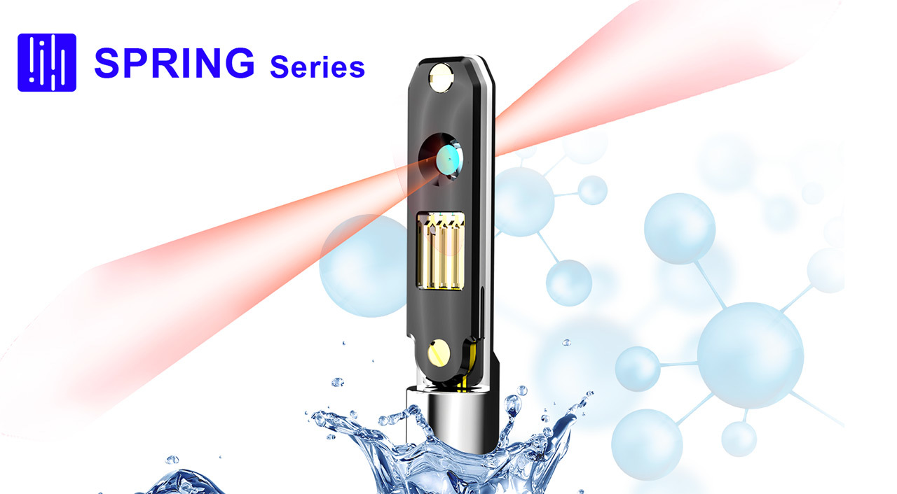
Spring Series In-Situ Holders(Optics)
Product Features
- Product composition
- Unique Advantages
- Functional Parameters
- Application
-
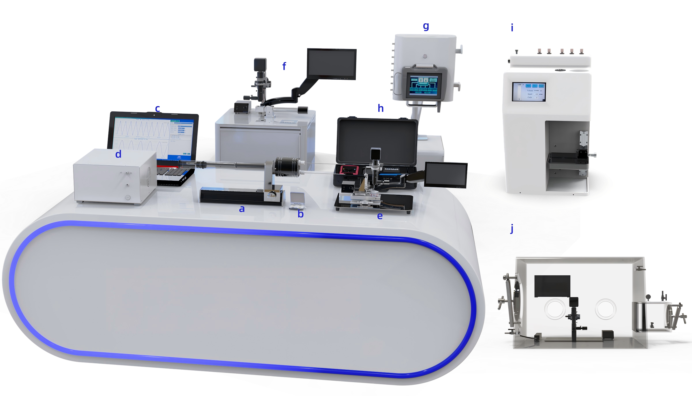
a.Spring Series In-Situ Holders(Optics) b.MEMS Liquid Optical Chip c.Light Source Control Program d.Light Source Workstation e.High-precision Chip Assembly Instrument f.High Vacuum Leak Checking Station g.In-situ Nanofluidic Control System (Liquid) h.Accessory Package i.Cleaning Instrument for Sample Holders j.Environment Gloves Box -
Highest resolution in the industry
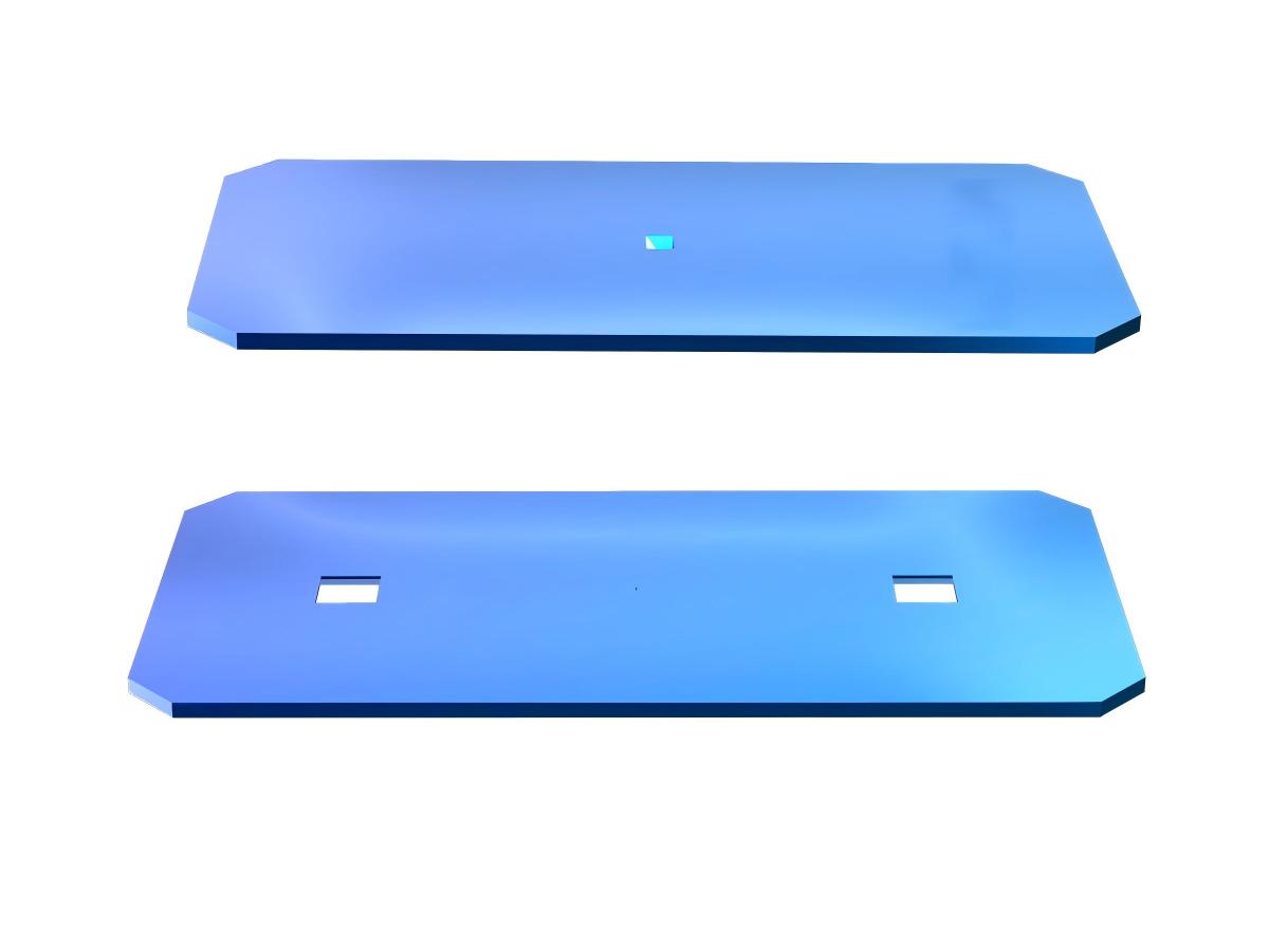
·1.Unique MEMS processing technology, with a silicon nitride film thickness of up to 10nm in the chip window area. ·2.The chip packaging adopts a dual-insurance method of bonding internal sealing and epoxy resin external sealing, making the interlayer between chips as thin as only about 100-200 nm. The ultra-thin interlayer greatly reduces interference with the electron beam, allowing clear observation of the atomic arrangement of the sample, and atomic-level resolution can be achieved in the liquid-phase environment. ·3.The specially designed shape of the chip window prevents the silicon nitride film from bulging, which would otherwise thicken the liquid layer and compromise resolution. High security ·1.Other common liquid sample holders from other brands on the market, due to the constraints of their own liquid cell chip design, can only use the high pressure generated by a liquid pump to drive a large flow of liquid through the sample stage and the peripheral area of the chip, posing a safety hazard of massive liquid leakage. The liquid mainly enters the nanochannels in the middle of the chip through the diffusion effect, and there is no real flow rate control in the chip's observation window. ·2.Nanofluidic control technology is employed, with fluid differential control implemented via a piezoelectric micro-control system to achieve nanoliter-scale trace fluid delivery. The residual liquid volume in both the in-situ nanofluidic control system and the sample rod is only at the microliter level, effectively ensuring the safety of the electron microscope. ·3.By adopting the polymer membrane surface contact sealing technology, compared with O-ring sealing, the sealing contact area is increased, which effectively reduces the risk of leakage. ·4.By adopting the ultra-high temperature coating technology, the silicon nitride film in the chip window area exhibits advantages such as high temperature resistance, low stress, pressure resistance, corrosion resistance, and radiation resistance. Unique multi-field coupling technology ·It can realize the multi-field coupling of light, electricity, heat, and fluid in a liquid-phase environment.
Excellent Optical Performance·1.Integrated laser light source, which integrates ultraviolet-visible-infrared bands and outputs laser with specific wavelengths. It features strong optical signals (maximum intensity not less than 150 mW/cm²), enables rapid and continuous adjustment of light source intensity, and has a short response time (millisecond level). ·2.Special structural design ensures ultra-low light loss, stable and uniform energy.
Intelligent Software and Automated Equipment·1.Man-machine separation is achieved: experimental conditions are remotely controlled via software, and detailed experimental data is automatically recorded throughout the entire process, facilitating experiment summary and review. ·2.Precision automated equipment is equipped throughout the whole workflow to assist manual operations and improve experimental efficiency. Team Advantages ·1.Team leaders participated in the development and completio
of in situ liquid phase TEM at the early stage of development.·2.The team independently designs in-situ chips and masters the core processes of chip manufacturing. ·3.With more than 20 members engaged in in-situ liquid-phase TEM research, the team can provide in-situ experimental technical support for multiple research directions. -
Category Index Functional Parameters Basic parameters Rod material High strength titanium alloy Window thickness 20nm(Support ugrande to 10nm) Applicable TEM brand Thermo Fisher/FEI, JEOL, Hitachi Applicable Pole Piece ST, XT, T, BioT, HRP, HTP, CRP Tilt Angle α=±20° (Actual range depends on electron microscope and pole piece model) (HR)TEM/STEM Supported (HR)EDS/EELS/SAED Supported -
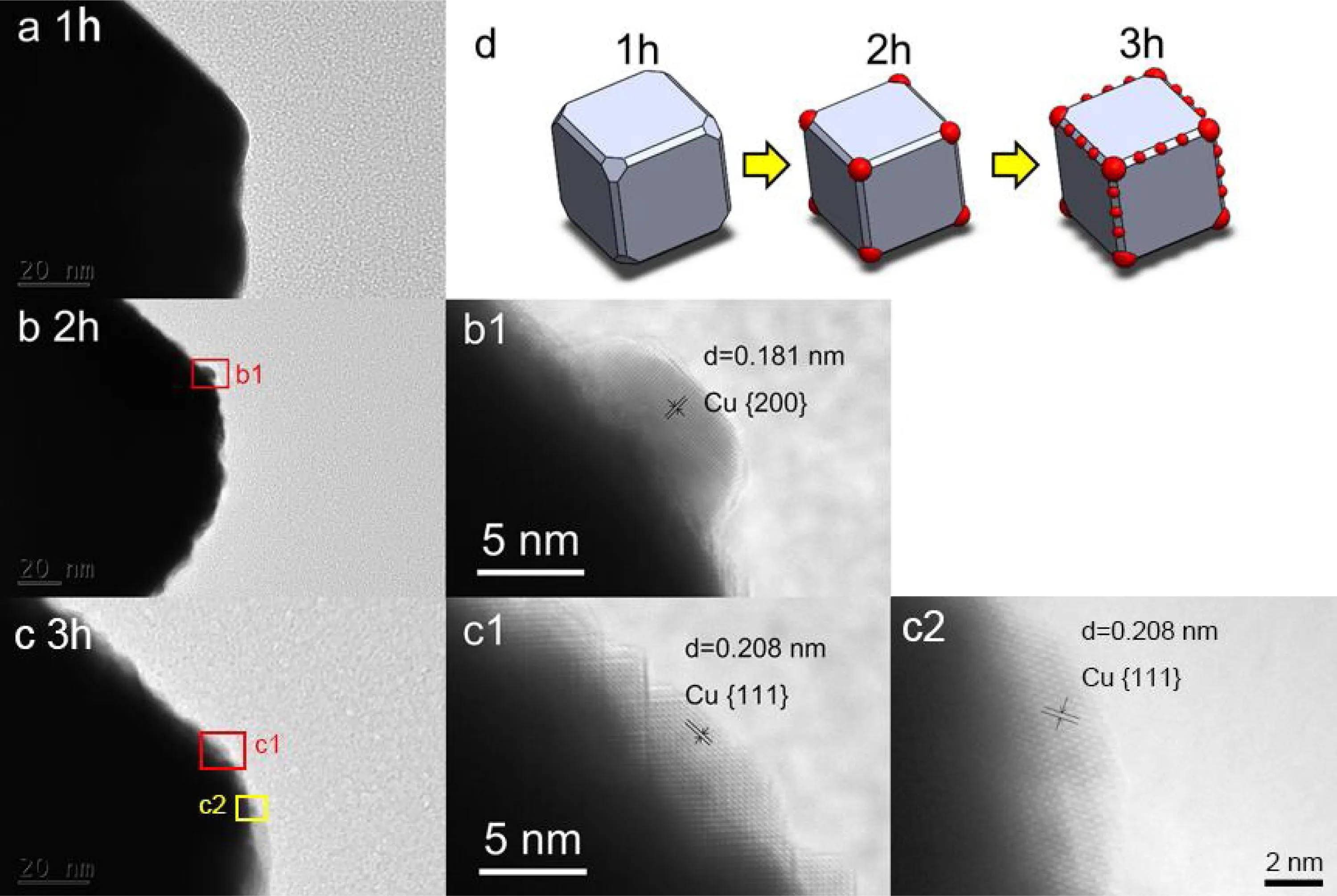
1、Photocatalysis:Recognition of surface active sites or site-specific reactions ,From Cu₂O to Cu during photoreduction.
Fig. 4. HRTEM images of Cu₂O samples with different irradiated time: (a) 1 h, (b) 2 h, (c) 3 h, and schematic diagrams of (d) Cu₂O structure change under
irradiation.Modified TEM holder with an optical fiber through it: (a, c) schematic diagrams, (b) real photo, and liquid cell chip: (d) schemat- ic diagram, (e) real photo.
Real time imaging of photocatalytic active site formation during H₂ evolution by in-situ TEM.
Applied Catalysis B Environmental, 2021, 284, 119743.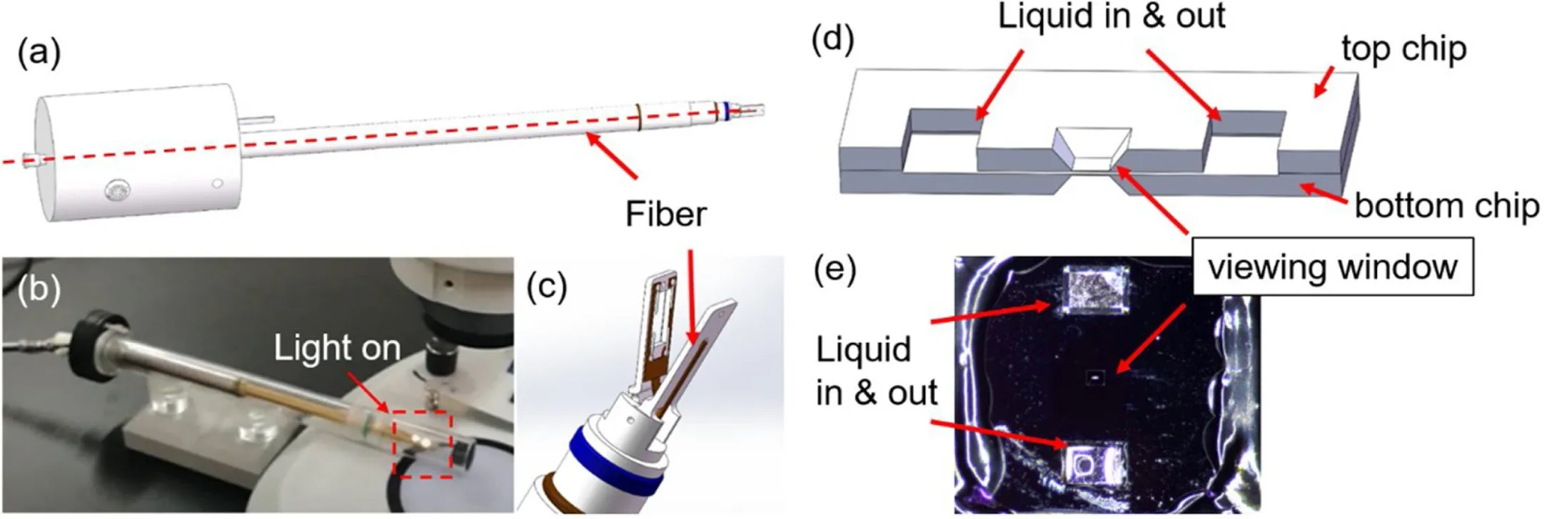
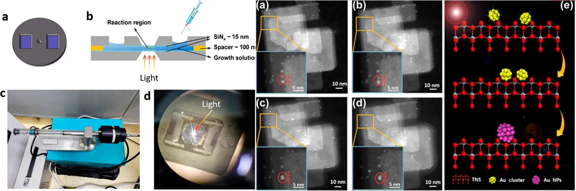
2、AResearch on Ultrasmall Gold (Au) Clusters in the Fields of Solar Energy Conversion and Photocatalysis
Figure 3 In situ STEM images before (a) and after 2 h (b), 4 h (c), 6 h (d) of UV–Vis light irradiation (220 nm < λ < 800 nm, 75 W Xe lamp with an energy output of 120 mW/cm²) under ambient conditions in air show the sintering behavior of Au clusters in TBA composites. Schematic illustration of the sintering mechanism of Au clusters under light illumination (e) .
Visualizing light-induced dynamic structural transformations of Au clusters-based photocatalyst via in situ TEM[J].
Nano Research, 2021, 14(8): 2805-2809.