

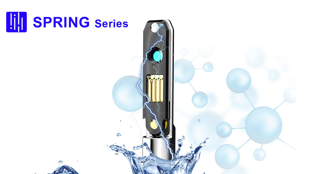
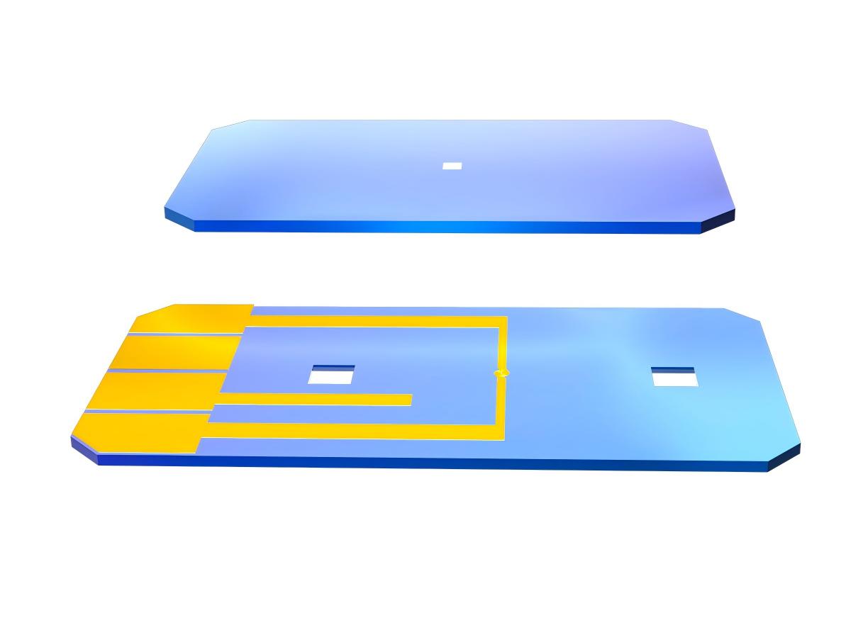
Spring Series In-Situ Holders(Electrochemistry)
Product Features
- Product composition
- Unique Advantages
- Functional Parameters
- Application
-
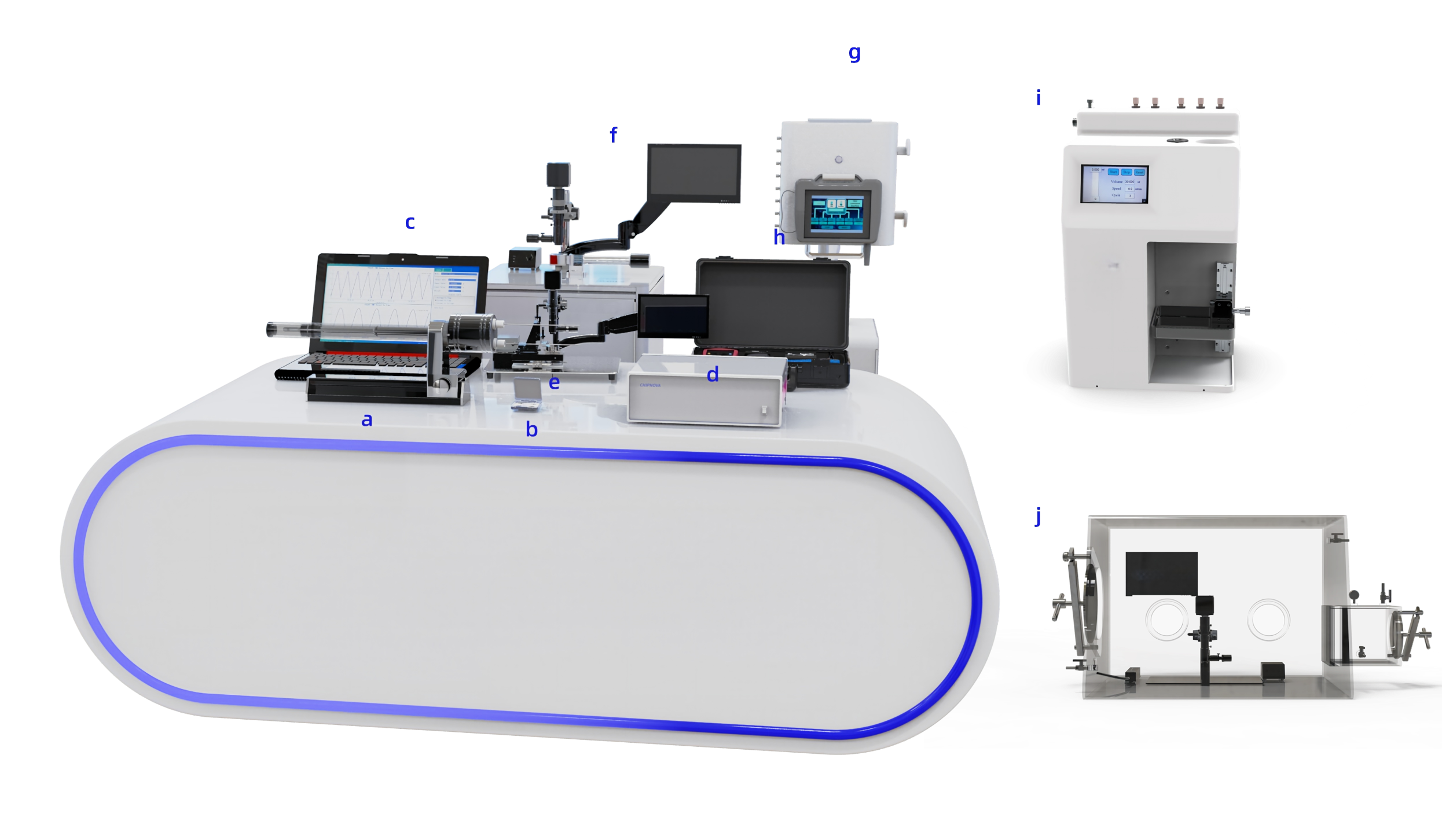
a.Spring Series In-Situ Holders(Electrochemistry) b.MEMS Electrochemistry Liquid Cell Chip (Static, Fluid) c.Electrical Control Software d.Electrochemical Workstation e.High-precision Chip Assembly Instrument f.High Vacuum Leak Checking Station g.In-situ Nanofluidic Control System (Liquid) h.Accessory Package i.Cleaning Instrument for Sample Holders j.Environment Gloves Box -
Highest resolution in the industry ·1.Unique MEMS processing technology, with a silicon nitride film thickness of up to 10nm in the chip window area. ·2.The chip packaging adopts a dual-insurance method of internal bonding and external epoxy resin sealing, making the interlayer between chips as thin as only about 100-200nm. The ultra-thin interlayer greatly reduces interference with the electron beam, allowing clear observation of the atomic arrangement of samples, and atomic-level resolution can be achieved in the liquid phase environment. ·3.The specially designed shape of the chip viewing window can avoid the bulging of the silicon nitride film that causes the liquid layer to thicken and affect the resolution. High security ·1.Other common liquid sample holders of other brands on the market, due to the constraints of their own liquid cell chip design, can only push large-flow liquid through the sample stage and the peripheral area of the chip by the huge pressure generated by the liquid pump, posing a safety hazard of large-scale liquid leakage. Their liquid mainly enters the nanochannel in the middle of the chip by diffusion effect, and there is no real flow rate control in the chip observation window. ·2.Nanofluidic control technology is employed, with fluid differential control implemented via a piezoelectric micro-control system to achieve nanoliter-scale trace fluid delivery. The residual liquid volume in both the in-situ nanofluidic control system and the sample rod is only at the microliter level, effectively ensuring the safety of the electron microscope. ·3.By adopting the polymer membrane surface contact sealing technology, compared with O-ring sealing, the sealing contact area is increased, which effectively reduces the risk of leakage. ·4.By adopting the ultra-high temperature coating technology, the silicon nitride film in the chip window area exhibits advantages such as high temperature resistance, low stress, pressure resistance, corrosion resistance, and radiation resistance. Unique Multi-Field Coupling Technology ·It can realize the multi-field coupling of light, electricity, heat, and fluid in a liquid-phase environment. Intelligent Software and Automated Equipment ·1.Man-machine separation is realized, where experimental conditions are remotely controlled by software, and detailed experimental data is automatically recorded throughout the process, facilitating summary and review. ·2.Precision automated equipment is equipped throughout the entire process to assist manual operations and improve experimental efficiency. Team Advantages ·1.Team leaders participated in the development and completio
of in situ liquid phase TEM at the early stage of development.·2.The team independently designs in-situ chips and masters the core processes of chip manufacturing. ·3.With more than 20 members engaged in in-situ liquid-phase TEM research, the team can provide in-situ experimental technical support for multiple research directions. -
Category Index Functional Parameters Basic parameters Rod Material High strength titanium alloy Window thickness 20nm(Support ugrande to 10nm) Applicable TEM brand Thermo Fisher/FEI, JEOL, Hitachi Applicable Pole Piece ST, XT, T, BioT, HRP, HTP, CRP Tilt Angle α=±20° (Actual range depends on electron microscope and pole piece model) (HR)TEM/STEM Supported (HR)EDS/EELS/SAED Supported -
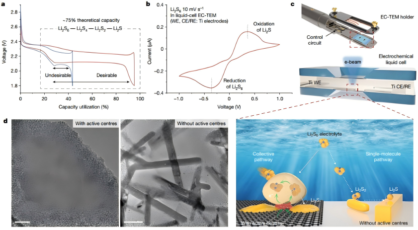
1. Published in Nature! A New Mechanism of Charge Storage-Aggregation Reaction at Battery Interfaces
Visualizing interfacial collective reaction behaviour of Li–S batteries.
Nature, 2023, 621, 75-81.文2、Driving the cell potential above a certain threshold potential during cycling leads to gas evolution that initiates a cascade of events, causing the active carbon to disintegrate.The first in situ transmission electron microscopy liquid cell design using an activated carbon substrate represents a breakthrough in understanding supercapacitor degradation, offering a working strategy for electrode dynamics investigation of various energy storage devices.
可Figure 3. Carbon electrode evolution of the ALD coated sample (a−d) under in situ CV test, (e−h) holding voltage at 1 V for 340 s. The line on the left is the edge of the deposited gold electrode, while the one on the right is the edge of the observe window.
Unveiling Activated Carbon Degradation in Supercapacitor Using Liquid Cell Transmission Electron Microscopy
ACS Appl. Energy Mater. 2024, 7, 9797−9805.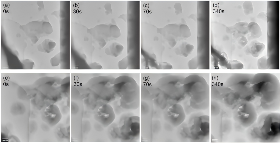
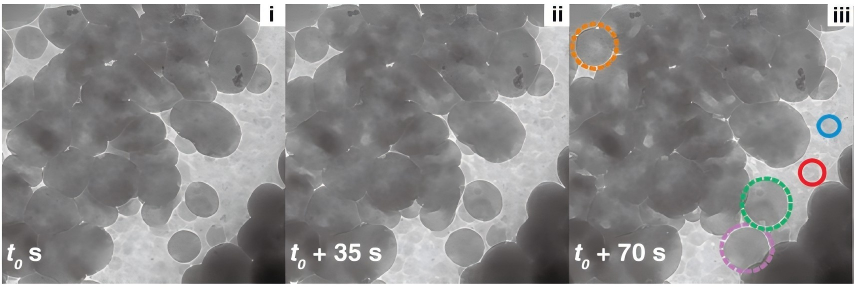
3.Nanoscale In - situ Observation of Li₂O₂ Growth
(b) Time-series TEM images during discharge of Li–O₂ in electrochemical liquid
cell. Scale bars in 500 nm.
Liquid cell electrochemical TEM: Unveiling the real-time interfacial reactions of advanced Li-metal batteries
J. Chem. Phys. 2022,157, 2309014.Fabrication of In - situ Electron Microscopy Liquid Cell
In Fig. 9 | In situ TEM observation of the lithiation and delithiation of MoS₂ nanosheets by using E-cell II (titanium/MoS₂ electrode, commercial LiPF₆/EC/DEC electrolyte). Top: sequential TEM images from Supplementary Videos 3 and 4, showing the SEI growth and MoS₂ decomposition process. Color is used to guide the eyes. Bottom:schematic illustration of SEI growth and MoS₂ decomposition process. Middle: section view of the E-cell at the imaging window, showing the internal environment of E-cell II and the SEI growth and MoS₂ decomposition phenomenon. The TEM images (top row) adapted with permission from ref. 23, American Chemical Society.
Fabrication of liquid cell for in situ transmission electron microscopy of electrochemical processes
Nature Protocols 2023,18, 555–578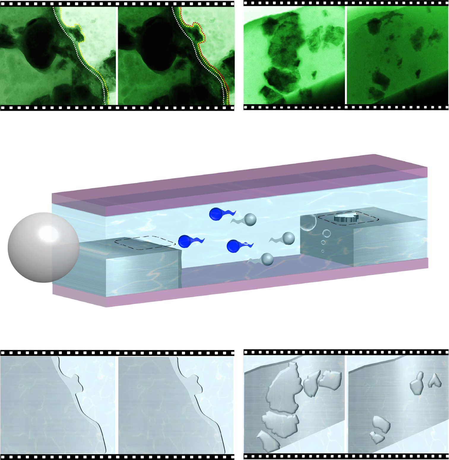
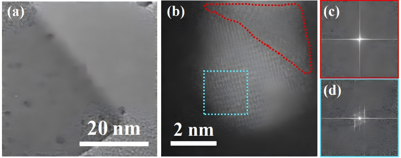
5.A novel electrocatalyst, Pt/α-PtOₓ/WO₃, was prepared, which provides a new insight for the design of high-performance metal-based catalysts—optimizing the reaction pathway by regulating the amorphous interface, and also offers a reference for the rational design of electrocatalysts.
Figure 2. High-resolution aberration-corrected STEM images of Pt NPs on the a) Pt/α-PtOx/WO₃, b) Pt/α-PtOx/WO₃-300, and c) Pt/α-PtOx/WO₃-400. The corresponding fast Fourier transform (FFT) pattern of the amorphous interface (a1), (b1), (c1) and crystal structure (a2), (b2), (c2) in the Pt NPs. The statistical ratio of crystalline Pt and amorphous PtOx for different Pt/α-PtOx/WO₃hybrids are shown in the inset of STEM images. d) High-resolution aberration-corrected STEM image of Pt NPs on the Pt/c-PtOx/WO₃ with crystal PtOx interface.
Engineering of Amorphous PtOx Interface on Pt/WO₃ Nanosheets for Ethanol Oxidation Electrocatalysis
Advanced Functional Materials ,2021, 31 (28)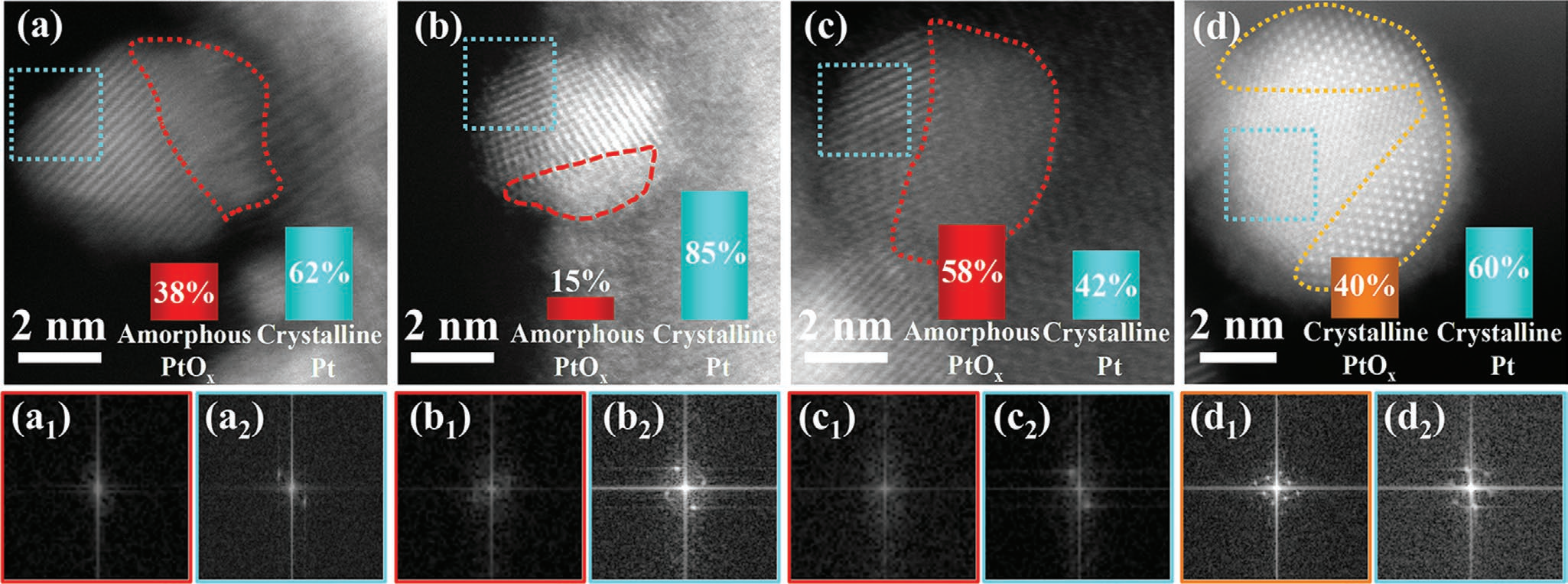
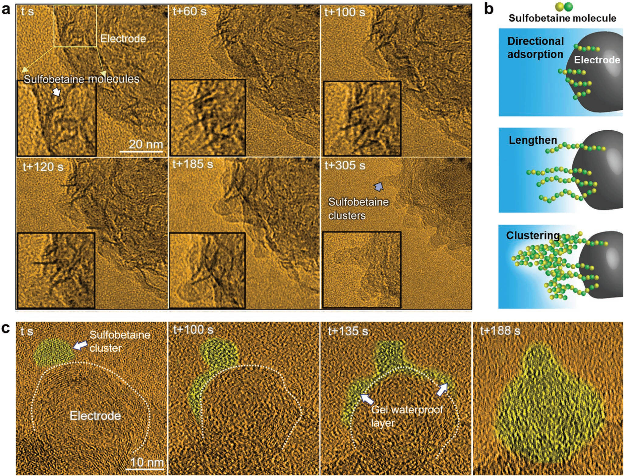
6. Electrochemistry: Under the action of an electric field, the evolution of sulfobetaine molecules at the solid-liquid interface and the formation of a water-repellent layer on the anode surface
Figure 2. In situ atomic resolution HRTEM observation on the behaviors of sulfobetaine molecules at the solid-liquid interface under external electric field and the formation of the waterproof layer around the negative electrode surface. a) The dynamic behaviors of sulfobetaine molecules and the formation of the gel clusters were observed. The time-series atomic resolution images show the change of morphology of the electrode and the NaNO₃–Sulfobetaine/H₂O electrolyte during the negative polarization process. b) Schematic of the formation of sulfobetaine waterproof layer through three major stages: attach, lengthen and clustering. c) A series of in situ HRTEM images showing the structural change of a single acetylene black particle with atomic resolution under negative charging. The gel clusters of sulfobetaine connected with each other and gradually paved around the surface of the electrode particle.
Controlling Interfacial Structural Evolution in Aqueous Electrolyte via Anti-Electrolytic Zwitterionic Waterproofing.
Advanced Functional Materials, 2022, 2207140.H